Electrical Engineering Services
Our goal is to be a seamless extension of your engineering team. FREEDOMCAD offers electrical engineering services for a variety of industries and applications. We will complement your electrical engineering team with technical services that add value to your operational processes. An array of capabilities enable us to be a one-stop solutions provider for all our customer’s electrical/electronic needs.
Electrical Engineering Specialists
FREEDOMCAD’s electrical engineering services have been employed in industries worldwide for a multitude of applications. Our quality management system, certified to ISO 9001:2015, to ensure that we can meet the strictest electrical and electronic specifications. We are also ITAR registered with the DDTC to service the Mil/Aero market.
To see how Freedom CAD’s electrical and electronic engineering services can benefit your operation, please contact us.
What Can FREEDOMCAD Provide for You?
Freedom CAD’s electrical engineering team possesses the expertise to meet your analog, digital and mixed signal circuitry needs. We specialize in areas such as field programmable gate array (FPGA) development, battery management, RF/wireless design, and microcontroller/DSP-based design, and high-speed digital circuitry and communications.
We can also provide prototypes and perform design validation testing, including environmental validation and agency testing & certification.
Additional Capabilities
Digital / High Speed Design
- Value Engineering
- Circuit Design & Analysis
- FPGA to ASIC Conversion
- DFx Analysis
- Test Planning (Design / Development)
- Component Analysis & Evaluation
- Compliance Engineering
Analog Design
- Data acquisition (Analog / Digital inputs)
- Signal Conditioning (Amplifiers / Filters)
- Pulsed Circuits (Linear / Non-linear)
- Control Systems
- Power Electronics
- Analog Circuit Simulation
Battery Management
- Value Engineering
- Circuit Design & Analysis
- FPGA to ASIC Conversion
- DFx Analysis
- Test Planning (Design / Development)
- Component Analysis & Evaluation
- Compliance Engineering
Thermal Management
- Value Engineering
- Circuit Design & Analysis
- FPGA to ASIC Conversion
- DFx Analysis
- Test Planning (Design / Development)
- Component Analysis & Evaluation
- Compliance Engineering
Case Studies

Battery Monitoring & Control Board
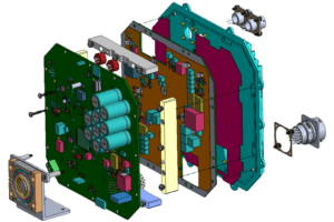
The Battery Monitoring & Control assembly included Electrical, Mechanical, Thermal, PCB Design, and 3D Printing for an Inductively Coupled, Galvanically Isolated Wireless Power Transfer application.
Design Features/Constraints
- Mill-Max Pogo Spring Pins and Pads for communicating from T-Clad to PCB
- 23 Pin Round Ethernet Connectors w/EMI Gasket Conn Pins Feed to Ethernet Mill-Max Pin Holders
- Faceplate & T-Clad is Pinned Diagonally to help Set Orientation
- 2x 5 Pin round Ethernet Connectors w/EMI Gaskets
- Conn Pins Feed to Ethernet Mill-Max Pin Holders
- Die Cut Conductive Thermal Gap Pad 3 W/m-K
- Exterior Faceplate Heatsink
- Wireless Power Transfer Assembly
- w/Flywire Pin Leads to Phoenix Conn

72 Line Infiniband Switch
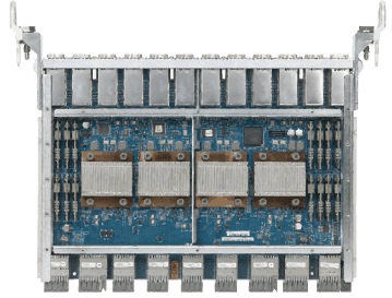
Goal: Reduce the cable count and complexity in highly integrated Infiniband switch systems. This approach was initially utilized to create a switching matrix as the heart of a supercomputer.
The main challenge in dealing with a design of this magnitude is the routing of high speed signals. To accommodate this challenge, routing groups had to be placed on different PCB layers separated by internal ground planes. This method would guarantee the reduction of crosstalk between signal groups. Signal groups consist of signal pairs coming to and from (Tx, Rx) the outside world (IPASS connectors), and signals coming to and from (Tx, Rx) the Fabric Card. Each layer has its own unique routing format to keep signal pairs from overlapping. Utilizing a Port Allocation Table facilitated a signal naming convention that enabled a more “route friendly” method for layout.

PCI Express (PCIe) Design
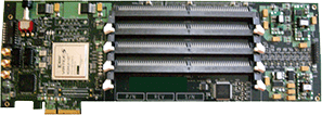
Goal: Engineer a RoHS compliant design that would fit within a four physical lane PCI Express (PCIe) form factor as defined in the PCIe 2.0 specification.
The Xilinx Virtex 5 FPGA device, part number XC5VLX85T-1FF1136C, was at the core of this design. Firmware and signal pin assignments for the FPGA were provided by the customer. A pair of external 200 MHz clock sources was required by the FPGA to internally generate the DDR and QDR memory clocks. At power on, the FPGA firmware was downloaded from the configuration SPI flash device. Following configuration the device allowed and controlled PCIe accesses to the on board DDR2 and QDR SRAM memory devices.
Memory consisted of four 22.5° DIMM sockets that support 2GB, 4GB, and 8GB DDR2 memory modules for a maximum total of 32GB of DDR2 memory. The memory modules support ECC and parity, and speeds from 266 MHz to 566 MHz. A single Samsung 8 MB QDR II SRAM device was also on board supporting 300 MHz clock speeds.
A manual reset switch was implemented to reset the FPGA as required during test. Further LED status indicators were provided for the following functions:
- Green/Red for each power source, green indicates power within limits, red indicates power out of limit
- Yellow for FPGA Load DONE complete
- Blue PCI link up
- 5 Green user defined indicators connected to the FPGA
Power supply voltages and currents were implemented for the following:
- DDR2 VREF 0.9V @ 6A
- VCCINT 1.0V @ 6A
- AVTTTX/RX 1.2V @ 4A
- AVCCPLL 1.2V @ 4A
- AVCC 1.0V @ 4A
- DDR2 1.8V @6A
- VCCO 2.5V @5A
- VCCAUX 2.5V @ 5A
- PCIVCC 3.3V @5A
The required voltages were created from the 3.3V and 12V power supplied over the PCIe bus. All voltages were monitored by a Lattice in-system programmable power supply monitoring, sequencing and margining controller. Freedom CAD engineers supplied the firmware for this device which also provided power on reset to the card.


