Why Use High Density Interconnect?
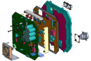
One of the fastest growing technologies in printed circuit board (PCB) design is high density interconnect (HDI). HDI boards allow for higher circuitry density than traditional circuit boards due to a more concentrated arrangement of smaller components, creating more concise pathways. Blind and/or buried vias are commonly used to optimize space in HDI boards, and microvias of .006 or less in diameter are now frequently used as well.
 A variety of verticals have incorporated HDI boards into their products, including manufacturers of military communications and strategic equipment, and medical diagnostic tools. The lightweight design of HDI boards also makes them ideal for aerospace applications and less bulky smartphones and laptops.
The most common types of HDI boards include:
- Through vias from surface-to-surface
- Combination through vias and buried vias
- Multiple HDI layers containing through vias
- A passive mounting substrate without any electrical connections
- Coreless construction through the use of layer pairs
- Alternate coreless constructions through the use of layer pairs
Benefits of HDI
For almost all applications pertaining to aeronautics, consumer products, computers, and electronics, HDI boards are not only suitable, but favored. Even in intense settings, HDI boards with multiple layers supply increased levels of reliability due to their powerful interconnection of stacked vias.
The reduction in the size of the components generates more space on which designers can work, opening up both sides of the raw PCB for design. Smaller components placed closer together produce additional input and output, allowing for quicker signal transmission and a substantial decline in crossing delays and signal loss.
HDI technology enables the reduction of an eight-layer through-hole PCB to a four-layer HDI microvia PCB, resulting in fewer layers that are capable of achieving equal or better functionality. This reduction considerably lowers material costs, making HDI technology very cost-effective for electronics manufacturers. The higher performance offered by multi-layer HDI PCBs make them reliable even in harsh environments.
Why Use HDI
Because of their light weight, reliable performance, and small size, HDI boards are especially appealing for wearable, mobile, and handheld electronics. Combined with the geometry of a high-density design, these stronger, smaller components and additional transistors elevate the function of a PCB and the end-product it is used for.
With components in closer proximity to one another, electrical signals take less time to travel. The high-density design of HDI boards reduces the rise time for the signal and the inductance, thus limiting the effects on nearby pins and leads. Additional transistors support not only increased functionality, but also heightened performance.
Concentrating on HDI design diminishes the time and cost of cultivating prototypes, shortening leads times, and allowing for much larger profit margins.
Learn More
HDI technology creates products that weigh less, perform faster and more efficiently, and come in smaller packages. The decrease in size enables the design of smaller end products that meet consumer demands for portability. HDI can be a time-consuming training endeavor for designers. But with increasing relevancy in the marketplace, the return in productivity, dependability, and fewer manufacturing delays renders the training time worthwhile.


